Category Archives: hardware

Review of Itead Sonoff Intelligent WiFi Socket

The intelligent WiFi mains socket is a device which is inserted into the original mains plug and has a mains socket itself. The mains output of the device can be controlled and switched on/off over an Internet connection.

The Itead Sonoff smart socket caught me with its simple design and with the possibility to upload custom firmware. The 10 amps socket is controlled by the WiFi capable ESP8266 microcontroller. ESP8266 is the leading platform for budget IoT devices. Its SDK is free and is well documented. It has built in WiFi, TCP/IP stack, free compiler and tools.

The device is produced by ITEAD studio, based in Shenzhen, China, website https://ww.itead.cc. The wiki product page is https://www.itead.cc/wiki/S20_Smart_Socket. In the Downloads section of this page https://www.itead.cc/wiki/S20_Smart_Socket#Downloads you can find the product schematics.

The socket comes in EU, US, UK, and China versions. This review covers the EU version of the socket, however most of the statements should be valid for the other versions.

The device comes packed into a solid cardboard box. The box is custom for the version of the smart socket and clearly shows how the specific plug looks like.

the box in which the socket is sold

The box in which the socket is sold


The box looks quite luxurious from inside. There is a cardboard piece which supports the plug and is probably also customized for the version of the socket as on this piece there is a profile of an EU plug.

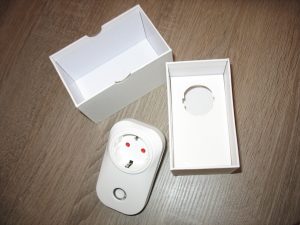
the socket unboxed

The socket unboxed

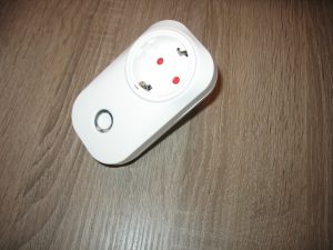
The external look shows a well built plastic case. The touch of the socket feels quite solid like an expensive device. The holes of the socket are fitted with child protection. There is a single button on the front of the socket.

front of the socket

Front of the socket

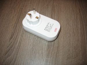
On the back of the socket there is an adjunct plug. On the plug there are explicit marks for L (line), N (null) and ⏚ (ground). A warranty seal with red Chinese inscription covers a hole with a screw which allows dismantling of the socket. A label reads:

WiFi Smart Power socket
Model: S20_EU
Input: AC 110 – 240V
Max Power: 2000W
Power Consuming: ≤ 0.3W

If we are not catchy for the funny English, the label is quite informative. As there is quite a wide voltage range, it seems the same schematics are used for all versions of the socket, and probably S20_EU is the EU version of the socket, S20_US is the US version of the socket, S20_UK is the UK version of the socket and S20_CN is the China version of the socket. The mains frequency 50 Hz or 60 Hz is not stated, as it is probably not important for the pulse switching power supply.

back of the socket

Back of the socket

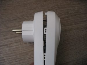
Now let’s look what is inside. We remove the warranty seal and undo the screw. Once you have undone the screw, there are several plastic locking fingers which have to pried

the socket pried from the side

The socket pried from the side

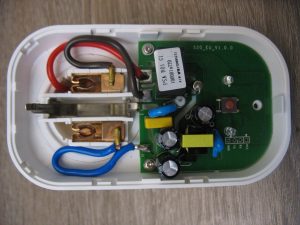
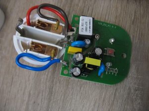
The firs look inside shows the wires are welded to the plug with electrical current. The pros for such welding are the high temperature and corrosion stability of the welding. The cons are that if the control of the welding is not good, weak electrical connection may occur.

The wiring looks quite neat. There is no foreseeable chance of a wire to melt down its isolation and to short circuit another wire, or a conducting surface to mechanically touch another conductive surface with the opposite potential. There are springs which create pressure for good electrical contact between the socket and the plugs which will be inserted. The discrete electronic components are well spaced from one another.

the front of the socket opened

The front of the socket opened

There is an inscription on the board which reads S20_EU_V1.0.0 . After all it seems that they use different boards for the EU, US, UK and China variants.
On the electrical relay there is a label which reads:

PSA B01 GL
100001a720
p/w: WWJG000627

The first line looks like a software version. The second line looks like a MQTT ID of the unit, and the third line is either a part number, or a password which allows access to the unit or with which the unit accesses a server.

The electronic board can be easily separated from the enclosure after undoing the two screws which support the board. The third screw which supports the board is the screw which is used to open the case of the socket and it has already been undone.

The socket board extracted

The socket board extracted

The power cables are soldered to the board. This is a point where weaknesses can appear, but with good control of the soldering this is OK. The cables conveniently keep the shape they had while in the enclosure, thus making the assembly to be easy.

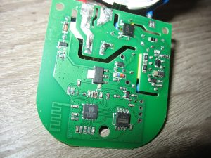
if we look at the back of the board, we see insulation channels cut in the board which keep the low voltage part of the board from the high voltage part. The power lines on the board are tinned in order to carry more current.

the back of the extracted socket board

The back of the extracted socket board

On the bottom we can see the ESP8266 chip with a label

ESP8266EX
482015
P48A17

The WiFi antenna can be seen in the bottom left of the picture.
In the bottom right can be seen an 8 Mbit, i.e.1MB, serial flash with label

winbond
25080BVSIG
1451L
.
This means the socket has plenty of space for firmware.

Let’s return to the front of the board.

serial port, programming

The serial port of the board

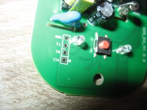
To the right of the button there is a RGB LED, which is used to indicate the status of the smart socket. To the left of the button there are 4 lines VCC, RX, TX and GND which can be used for programming. The button itself is connects GPIO0 of ESP8266EX to the ground, so when the board is powered while the button is pressed, ESP8266 enters programming mode and new firmware can be flashed.

In the upper right corner we can see a 10 A fuse which is meant to protect the high-power circuit in case of current overload.

Finally let’s look at the power relay.

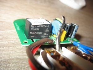
the relay of the socket, HF32FA-G, 10A, 250VAC

The relay of the socket

The relay has a label
HF32FA-G
005-HS2
10A 250VAC
CHINA FP0412B

The 10A of the relay give a little safety factor of 10% over the advertised switching power of 2000 W for 220 V mains voltage. To stay on the safe side, I would use the power socket for loads of up to 1000 W.

I purchased the socket from Aliexpress https://www.aliexpress.com/item/Itead-Sonoff-Wif-Wireless-Remote-Control-Switch-Smart-Home-10A-16A-Universal-intelligent-DIY-Timer-Switch/32760053192.html , for $16.70, with shipping via Singapore Post for $1.73. The item was dispatched and delivered very quickly.

If you want to gain experience with ESP8266 there is a free SDK, documentation, cheap hardware modules and plenty of programming examples freely available in Github and other sites.

Belkin F6D6230-4 v1 Teardown

I recently bought a Belkin F6D6230-4 v1, also known as F6D6230uk4, router from eBay UK for £15.99, with free P&P. The router came with its original box, original polyethylene protecting film and looked like new.

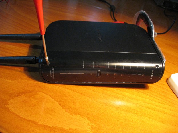
IMG_3716I had read some really negative comments about this model, so I decided to change its firmware with OpenWRT or DDWRT firmware. I spend an evening looking for a successful installation of such firmware, but I didn’t come upon any. The devil, though black and horned, as you can see on the photo, is sometimes not so evil, so I decided to start looking a way to get enough information to port such firmware on it. The first step is to make a research information is available on the internet for that particular model. The second step is to make a tear-down of the hardware in order to see the hardware, and the third step is to make the actual port, or to assist to some person who is responsible for porting the firmware to new router models.

in the first step of the research, I came to the WikiDevi page for this model. this model comes with 8 MB flash memory, 64 MB RAM, BCM4718A1 CPU, in which is integrated the 2.4 GHz radio, and BCM43224 in which is integrated the 5 GHz radio. The router comes also with 1 USB port, 4 LAN ports and 1 WAN port, with a BCM53115 switch chip.

The Teardown

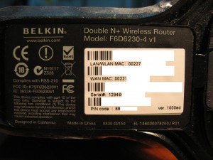
Let’s see the label. The private information is removed.

Label of Belkin F6D6230-4 v1, private information is removed

Label of Belkin F6D6230-4 v1, private information is removed

Now let’s have a look inside. There are two hidden screws under the front panel cover. There are two approaches to unscrew the screws. You can either peel the front panel cover off, or just make holes into it. I preferred the second approach.

F6D6230-4 hidden screws

F6D6230-4 hidden screws

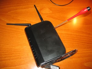
After that the top cover must be priced:

Pricing of the top cover

Pricing of the top cover

Below is given a photo of what we see inside.

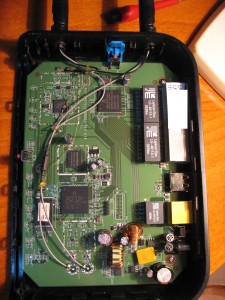
Belkin F6D6230-4 v1 inside

Belkin F6D6230-4 v1 inside

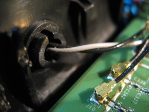
The first things which comes to my attention is that we see that the antennas are used for both 2.5 GHz and 5 GHz bands. Each antenna is fed with 2 coax cables. One of the cables is white and the other cable is black. The white cables seem to be used for 2.4 Ghz, while the black cables are probably used for 5 GHz signals. This brings the question of how efficient the antennas are. Usually combining 2 different bands lowers the efficiency of the antennas. I will leave this question open and will not dismantle the antennas for now.

The antenna attachment

The antenna attachment, You can see both coax cables.

Both antennas are attached permanently. It is not possible to change the antennas without changing the design of the router.

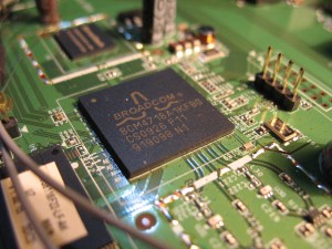
Near the main chip BCM4718A is the serial port connector, and a port for which no pins are soldered, most probably the JTAG connector. You will find how to use the serial connector in the next article of the series for Belkin F6D6230-4.

BCM4718A, serial port connector and JTAG

BCM4718A, serial port connector and JTAG

Another view of the chip, the serial connector and the JTAG:

BCM4718A, serial port connector and JTAG - another view

BCM4718A, serial port connector and JTAG – another view


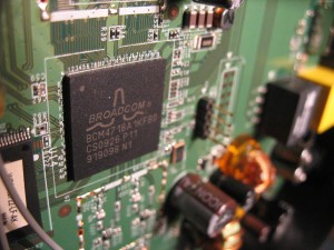
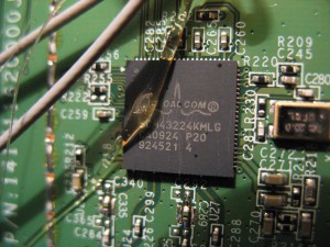
The 5 GHz radio chip is Broadcom BCM43224KMLG. It has a separate quartz oscilator.

BCM43224

BCM43224

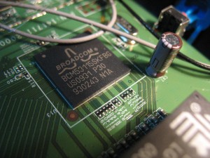
The 5-port ethernet switch chip BCM53115SKFBG is said in its product brief to be for speed 10/100/1000 Mbps. Together with the line transformers LG-4811X-1 it sets the Ethernet speed to 1000 Mbps.

BCM53115SKFBG

The ethernet switch chip BCM53115SKFBG

The antenna cables are interestingly born by soldered pins.

Antenna cable bearings

Antenna cable bearings

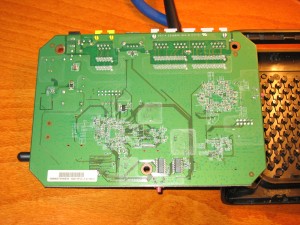
The back side of the board is less interesting:

F6D6230 back side of the board

F6D6230 back side of the board

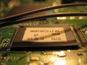
Flash memory of Belkin F6D6230

Flash memory of Belkin F6D6230

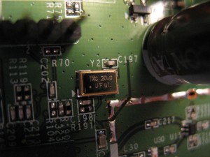
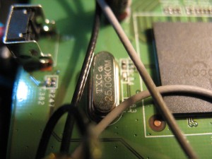
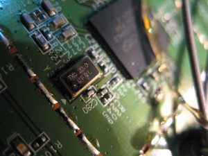
There are 3 quartz oscillators for the three main chips:

Quartz oscilator for BCM4718A


Quartz oscilator for BCM53115

Quartz oscilator for BCM53115

Quartz oscillator for BCM43224

Quartz oscillator for BCM43224

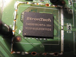
The RAM memory is EnronTech EM68B16CWPA-25H, 32 M x 16 bit, DDR2, 400 MHz.


EM68B16CWPA-25H

EM68B16CWPA-25H

Interesting notice

I noticed something very interesting while playing with the router. The main chip BCM4718A gets very hot. When I put my finger on the chip, I almost feel pain, which means the temperature is over 60 degrees Celsius, about 140 degrees Fahrenheit, which is the temperature threshold for feeling pain. Many of the complaints for this router are related to the system stability, and it is very likely the poor stability is related with the overheating of the central processor, which works in synergy with the poor firmware.

Conclusion

The system parameters of this router look quite good, its price is just right for its current firmware suport, but for the future the device seems a bit underestimated. I hope that with a heatsink for the BCM4718A chip and an open source firmware, this router will become a pearl in the crown in my home network.


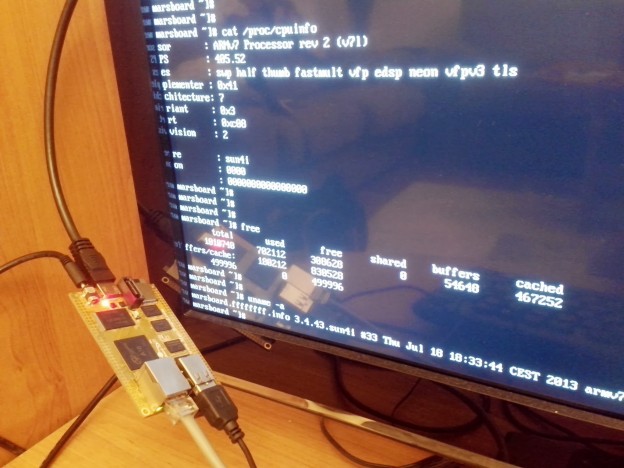
Fedora 19 running on Marsboard A10 on my TV

Running Fedora 19 on Marsboard A10

I recently purchased a Marsboard A10 development board from the Shenzhen based company HAOYU Electronics. The shipment to Bulgaria took less than 2 weeks via Hongkong post. On the Marsboard’s site there are some links to software, which can be used, a wiki page, and a forum about the board, however I had to successfully deal with some troubles when trying to use the solutions provided.

The board is advertised as being open, however not all issues about compilation and installation of software are clearly explained. Some images were not able to boot, the provided versions of the software were too old, e.g. Android version 4.0.4, Ubintu 12.06. The Linaro ubuntu distribution from the downloads page of Marsboard web site was running at very low frequency, with no change under heavy loads, probably due to poor bootloader configuration.

I noticed in this post that a Fedora 19 distribution for Cubieboard and other ARM boards was released. Cubieboard is very similar to Marsboard. I decided to try to adapt it to Marsboard A10.

As described in the  README file of the distribution, after the image is copied to an SD card, a script select-board.sh from the boot partition must be run, in order to install the u-boot bootloader and the boot configuration for the particular board:

cd ~/Downloads/Marsboard
wget http://scotland.proximity.on.ca/contrib-images/hansg/Fedora-19-a10-armhfp-r1.img.xz
wget http://scotland.proximity.on.ca/contrib-images/hansg/README-F19
xzcat Fedora-19-a10-armhfp-r1.img.xz >Fedora-19-a10-armhfp-r1.img

Now make sure the SD card on which you want to install the image has volume least 8 GB, that the SD card is inserted in the reader,  and that it is /dev/mmcblk0, now copy the image to the SD card

dd if=Fedora-19-a10-armhfp-r1.img of=/dev/mmcblk0 bs=4096 count=1926144
sync

The sync-ing flushes the cached information cached in memory to the physical medium. You may notice that it takes time, as a big part of the file was cached in the memory. After the sync command finishes, take out and re-insert the SD card. If you do this before the sync command has finished, the information saved on the SD card will become corrupt.

The problem was that the Marsboard board was not present in the list of the boards. I had to compile u-boot for Marsboard A10, accommodate the configurations for Marsboard, create a sub-directory for Marsboard under the boards/sun4i directory, and add the Marsboard profile in the select-board.sh script.

For each board with sun4i architecture there is a directory boards/sun4i/BOARDNICKNAME, where BOARDNICKNAME is the nickname of the board as defined in the select-board.sh script, used for identifying the board. There are u-boot.bin and sunxi-spl.bin files, which are part of u-boot, BOARDNICKNAME.fex file, with configuration parameters for the board, and a script.bin file, which is produced from BOARDNICKNAME.fex file using the fex2bin tool received from

mkdir -p ~/Downloads/Marsboard
git clone https://github.com/linux-sunxi/sunxi-tools
cd sunxi-tools
make clean
make
./fex2bin BOARDNICKNAME.fex >script.bin

So I’ll prepare a directory in which I’ll collect the files needed:

mkdir ~/Downloads/Marsboard/f19-boards-marsboard

Follow the instruction in the How to compile u-boot for Marsboard A10 article. After the compilation, copy the needed files in the prepared directory above:

cp u-boot.bin spl/sunxi-spl.bin ~/Downloads/Marsboard/f19-boards-marsboard

Now we need the marsboard.fex and script.bin files. From the marsboard-android-4.0.4-sdk.7z archive we can find the .fex file, as this post suggests.

cd ~/Downloads/Marsboard
wget http://www.haoyuelectronics.com/marsboard/marsboard-android-4.0.4-sdk.7z
7z l marsboard-android-4.0.4-sdk.7z
7z x marsboard-android-4.0.4-sdk.7z
find marsboard-android-4.0.4-sdk -name '*.fex'

There are 2 files which can be the corect files:

./marsboard-android-4.0.4-sdk/tools/pack/chips/sun4i/configs/crane/marsboard/sys_config1.fex
./marsboard-android-4.0.4-sdk/tools/pack/chips/sun4i/configs/crane/marsboard/sys_config.fex

By comparison of the files with the *.fex files from the uboot partition of the Fedora 19 image, e.g. we can find that sys_config1.fex is the correct *.fex file to copy to the board directory.

cp ./marsboard-android-4.0.4-sdk/tools/pack/chips/sun4i/configs/crane/marsboard/sys_config1.fex ./f19-boards-marsboard/marsboard.fex

Now translate the fex file to script.bin:

./sunxi-tools/fex2bin ./f19-boards-marsboard/marsboard.fex >./f19-boards-marsboard/script.bin

Remember that we left the SD card with the Fedora 19 image re-inserted, and the 1 and 3 partitions, labelled uboot and rootfs are mounted automatically to /run/media/$USERNAME/uboot and /run/media/$USERNAME/rootfs, where $USERNAME is the environment variable, which contains your username. Now copy the f19-boards-marsboard to the sun4i directory:

cp -R ./f19-boards-marsboard /run/media/$USERNAME/uboot/boards/sun4i/marsboard

Now what is left is to add marsboard in the select-board.sh script. This happens with only one line, marked below with ‘+’ to show the difference:

 BOARDS+=(wobo-i5             "Wobo i5 TV Box")
 BOARDS+=(xzpad700            "XZPAD700 7\" tablet")
+BOARDS+=(marsboard           "Marsboard A10")

 if [ "$1" = "--help" -o -z "$DIALOG" -a -z "$BOARD" ]; then
     echo "Usage: \"$0 <board>\""

In the real select-board.sh the + in the start of the line should not exist. Now sync the changes and umount the filesystems from the SD card:

sync
umount /run/media/$USERNAME/uboot /run/media/$USERNAME/rootfs

Now you can unplug the SD card from the card reader, plug it in the Marsboard, and enjoy your Fedora 19 installation.

Fedora 19 running on Marsboard A10 on my TV

Fedora 19 running on Marsboard A10 on my TV

You can find an archive with the files produced here: Fedora 19 on Marsboard A10 bootfiles

How to compile u-boot for Marsboard A10

The next instruction is for cross-compiling the u-boot bootloader for Marsboard A10 on Fedora 19 x86_64. With little modifications it should be able to work with other versions of Fedora, and to compile u-boot for another ARM board, e.g. Marsboard A20, ot Cubieboard.

Make sure the arm-linux-gnu toolchain is installed

yum install gcc-arm-linux-gnu binutils-arm-linux-gnu

My exact versions of those 2 packages are

# rpm -qa | grep arm-linux
gcc-arm-linux-gnu-4.7.2-2.aa.20121114svn.fc19.1.x86_64
binutils-arm-linux-gnu-2.23.51.0.3-1.fc19.x86_64

Please note that I tried the arm-none-eabi toolchain, but I encountered a problem during the cross-compilation. The cross-compilation was failing with segmentation fault, so I switched to arm-linux-gnu toolchain.

The command line of the instruction from the wiki How to compile the Allwinner A10 u-boot

git clone git://github.com/hno/uboot-allwinner.git

is not working, as the uboot-allwinner repository was removed.
I found that in the main u-boot repository there was a recent addition of Marsboard A20. The Marsboard A10 configuration for u-boot was present too. So I cloned the repository locally:

mkdir -p ~/Downloads/Marsboard
cd ~/Downloads/Marsboard
git clone git://github.com/hno/u-boot.git
cd u-boot

According to the README file in the u-boot root directory, after I found that the name of the board is Marsboard_A10 in the u-boot configuration lists, the next instructions had to compile u-boot:

export CROSS_COMPILE=arm-linux-gnu-
make Marsboard_A10_config
make clean
make

Don’t forget the trailing dash ‘‘ of the arm-linux-gnu- string which is put into the CROSS_COMPILE variable.

If everything compiled fine, you’ll have the u-boot.bin file in the root of the u-boot tree, and sunxi-spl.bin in the spl/ directory.

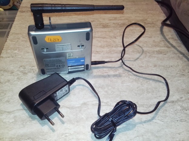
WRT54GC with its power supply

How to repair faulty WRT54GC power supply adapter

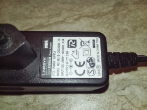
WRT54GC power supply label

WRT54GC power supply label. A good reason to repair the power supply is that 3.3V 2A adapter is difficult to find.

WARNING: Mishandling the repair of any power unit can lead to electric shock or fire, which can kill you or somebody else, or produce damage. Do not attempt this repair unless you are qualified for the task.

Now that you have been warned I can continue with the rest.

I’ve had a total 4 cases of failure of power supply adapters of Linksys WRT54GC routers for 4.5 years for 2 such routers. The first three failures were covered by the warranty, so what I had to do was just take the failed power adapters together with the routers to the service company. They replaced the faulty power units with working ones.

The last failure happened several months ago. I found the router had a trend to hang more and more frequently. The power unit was getting extremely hot and the WRT54GC router which was powered by it was failing. I had handy a unit from another WRT54GC router, so I tested the router with it. It was clear that it was the next power unit failure in the series. It seems to me that the power units were either misdesigned, or low grade components were used.

I saw that the warranty has expired. I had had quite good experience with various electronic devices, so I decided to repair the faulty WRT54GC power unit myself. The unit was sealed either by glue or by melting at high temperature, so I had to cut the line where the front and the back parts of the case join, using a thin saw, and then eventually with a cutter blade. Knowing that I can damage any internal parts I was extremely careful doing that operation.

I split the front from the back of the power unit. I carefully discharged all the capacitors, just in case they had remained charged. After all, the inut circuit was powered by AC about 220 V and I didn’t want to get hurt. After that I started to inspect the circuit.

As I could imagine, at least one of the electrolyte capacitors had failed. It had become swollen. Using a solder and a desoldering pump, I removed it and replaced it with a higher grade capacitor with slightly higher maximum voltage and the same capacity. It was a bit bigger but it fit into the footprint of the case.

I closed the case and fastened it with PVC band. I could alternatively seal the case using a solder to melt the plastic where the edges join together. The good attachment is extremely important in environments where children can reach the power adapter. My power unit is put of the reach of children, it remained fastened with PVC band.

I tested the power supply. The router was working just fine. The power unit was not too hot, so I did not need to use alternative means of attachment or to make holes in order to improve heat dissipation.

I am sorry I did not take photos during the repair works, but  I hope the verbal description of the task was a sufficient tip on how to repair the power unit and enjoy more years with your WRT54GC. 🙂

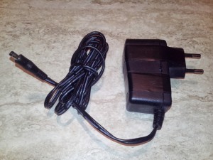
The repaired WRT54GC power supply

The repaired WRT54GC power supply

Regards,
Nikolay